- 您现在的位置:买卖IC网 > Sheet目录1917 > DSPIC30F3013-20I/ML (Microchip Technology)IC DSPIC MCU/DSP 24K 44QFN
PIC18F46J11 FAMILY
DS39932D-page 134
2011 Microchip Technology Inc.
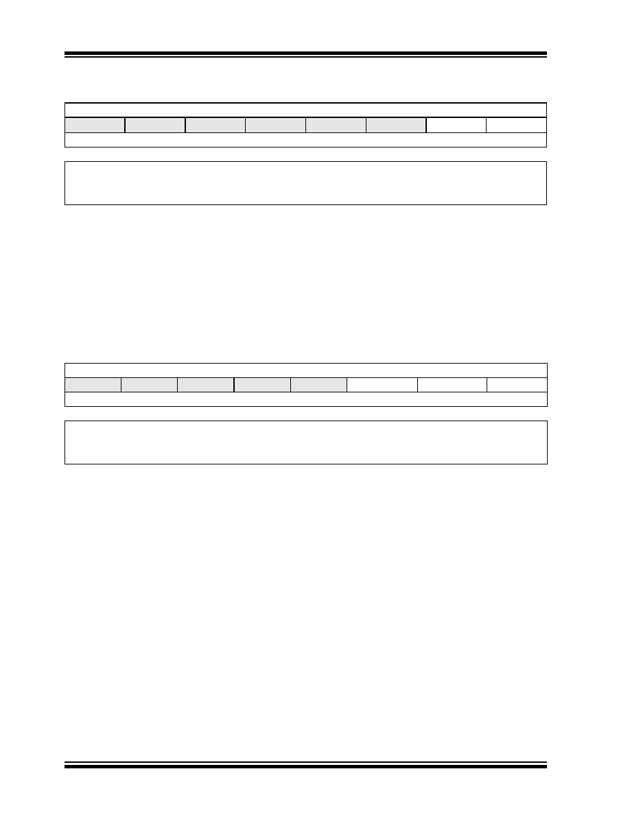
REGISTER 10-3:
ODCON3: PERIPHERAL OPEN-DRAIN CONTROL REGISTER 3 (BANKED F40h)
U-0
R/W-0
—
SPI2OD
SPI1OD
bit 7
bit 0
Legend:
R = Readable bit
W = Writable bit
U = Unimplemented bit, read as ‘0’
-n = Value at POR
‘1’ = Bit is set
‘0’ = Bit is cleared
x = Bit is unknown
bit 7-2
Unimplemented:
Read as ‘0’
bit 1
SPI2OD:
SPI2 Open-Drain Output Enable bit
1
= Open-drain capability enabled
0
= Open-drain capability disabled
bit 0
SPI1OD:
SPI1 Open-Drain Output Enable bit
1
= Open-drain capability enabled
0
= Open-drain capability disabled
REGISTER 10-4:
PADCFG1: PAD CONFIGURATION CONTROL REGISTER 1 (BANKED F3Ch)
U-0
R/W-0
—
RTSECSEL1(1) RTSECSEL0(1)
PMPTTL
bit 7
bit 0
Legend:
R = Readable bit
W = Writable bit
U = Unimplemented bit, read as ‘0’
-n = Value at POR
‘1’ = Bit is set
‘0’ = Bit is cleared
x = Bit is unknown
bit 7-3
Unimplemented:
Read as ‘0’
bit 2-1
RTSECSEL<1:0>:
RTCC Seconds Clock Output Select bits(1)
11
= Reserved; do not use
10
= RTCC source clock is selected for the RTCC pin (can be INTRC or T1OSC, depending on the
RTCOSC (CONFIG3L<1>) setting)
01
= RTCC seconds clock is selected for the RTCC pin
00
= RTCC alarm pulse is selected for the RTCC pin
bit 0
PMPTTL:
PMP Module TTL Input Buffer Select bit
1
= PMP module uses TTL input buffers
0
= PMP module uses Schmitt Trigger input buffers
Note 1:
To enable the actual RTCC output, the RTCOE (RTCCFG<2>) bit needs to be set.
发布紧急采购,3分钟左右您将得到回复。
相关PDF资料
DSPIC30F4011-30I/ML
IC DSPIC MCU/DSP 48K 44QFN
DSPIC30F4013-30I/ML
IC DSPIC MCU/DSP 48K 44QFN
DSPIC30F5013-30I/PT
IC DSPIC MCU/DSP 66K 80TQFP
DSPIC30F5015-30I/PT
IC DSPIC MCU/DSP 66K 64TQFP
DSPIC30F6010-20E/PF
IC DSPIC MCU/DSP 144K 80TQFP
DSPIC30F6010A-30I/PF
IC DSPIC MCU/DSP 144K 80TQFP
DSPIC30F6013A-30I/PF
IC DSPIC MCU/DSP 132K 80TQFP
DSPIC30F6014-30I/PF
IC DSPIC MCU/DSP 144K 80TQFP
相关代理商/技术参数
dsPIC30F3013-20I/SO
功能描述:数字信号处理器和控制器 - DSP, DSC 28LD 20MIPS 24 KB RoHS:否 制造商:Microchip Technology 核心:dsPIC 数据总线宽度:16 bit 程序存储器大小:16 KB 数据 RAM 大小:2 KB 最大时钟频率:40 MHz 可编程输入/输出端数量:35 定时器数量:3 设备每秒兆指令数:50 MIPs 工作电源电压:3.3 V 最大工作温度:+ 85 C 封装 / 箱体:TQFP-44 安装风格:SMD/SMT
dsPIC30F3013-20I/SP
功能描述:数字信号处理器和控制器 - DSP, DSC 28LD 20MIPS 24 KB RoHS:否 制造商:Microchip Technology 核心:dsPIC 数据总线宽度:16 bit 程序存储器大小:16 KB 数据 RAM 大小:2 KB 最大时钟频率:40 MHz 可编程输入/输出端数量:35 定时器数量:3 设备每秒兆指令数:50 MIPs 工作电源电压:3.3 V 最大工作温度:+ 85 C 封装 / 箱体:TQFP-44 安装风格:SMD/SMT
DSPIC30F3013-30I/ML
功能描述:数字信号处理器和控制器 - DSP, DSC Sensor RoHS:否 制造商:Microchip Technology 核心:dsPIC 数据总线宽度:16 bit 程序存储器大小:16 KB 数据 RAM 大小:2 KB 最大时钟频率:40 MHz 可编程输入/输出端数量:35 定时器数量:3 设备每秒兆指令数:50 MIPs 工作电源电压:3.3 V 最大工作温度:+ 85 C 封装 / 箱体:TQFP-44 安装风格:SMD/SMT
DSPIC30F3013-30I/SO
功能描述:数字信号处理器和控制器 - DSP, DSC Sensor RoHS:否 制造商:Microchip Technology 核心:dsPIC 数据总线宽度:16 bit 程序存储器大小:16 KB 数据 RAM 大小:2 KB 最大时钟频率:40 MHz 可编程输入/输出端数量:35 定时器数量:3 设备每秒兆指令数:50 MIPs 工作电源电压:3.3 V 最大工作温度:+ 85 C 封装 / 箱体:TQFP-44 安装风格:SMD/SMT
DSPIC30F3013-30I/SO
制造商:Microchip Technology Inc 功能描述:IC DSC 16BIT 24KB 40MHZ 5.5V SOIC-28
DSPIC30F3013-30I/SP
功能描述:数字信号处理器和控制器 - DSP, DSC Sensor RoHS:否 制造商:Microchip Technology 核心:dsPIC 数据总线宽度:16 bit 程序存储器大小:16 KB 数据 RAM 大小:2 KB 最大时钟频率:40 MHz 可编程输入/输出端数量:35 定时器数量:3 设备每秒兆指令数:50 MIPs 工作电源电压:3.3 V 最大工作温度:+ 85 C 封装 / 箱体:TQFP-44 安装风格:SMD/SMT
DSPIC30F3013-30I/SP
制造商:Microchip Technology Inc 功能描述:16-Bit Digital Signal Controller
dsPIC30F3013T-20E/ML
功能描述:数字信号处理器和控制器 - DSP, DSC 44LD 20MIPS 24 KB RoHS:否 制造商:Microchip Technology 核心:dsPIC 数据总线宽度:16 bit 程序存储器大小:16 KB 数据 RAM 大小:2 KB 最大时钟频率:40 MHz 可编程输入/输出端数量:35 定时器数量:3 设备每秒兆指令数:50 MIPs 工作电源电压:3.3 V 最大工作温度:+ 85 C 封装 / 箱体:TQFP-44 安装风格:SMD/SMT